STM |
您所在的位置:网站首页 › stm32 dma传输速度 › STM |
STM
|
目录
一、前言二、SPI功能框图三、SPI通信读写数据四、硬件SPI读写W25Q644.1接线图4.2程序代码
一、前言
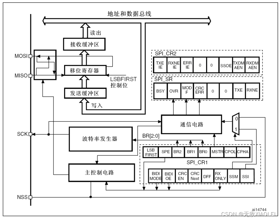
STM32的SPI外设可用作通讯的主机及从机,支持最高的SCK时钟频率为fpclk/2 (STM32F103型号的芯片默认 fpclk1为 36MHz,fpclk2为 72MHz),完全支持 SPI协议的4种模式,数据帧长度可设置为8位或16位,可设置数据 MSB先行或 LSB 先行。它还支持双线全双工、双线单向以及单线模式。其中双线单向模式可以同时使用 MOSI及 MISO 数据线向一个方向传输数据,可以加快一倍的传输速度。而单线模式则可以减少硬件接线,当然这样速率会受到影响。 二、SPI功能框图
MISO:主设备输入/从设备输出引脚。该引脚在从模式下发送数据,在主模式下接收数据。 MOSI:主设备输出/从设备输入引脚。该引脚在主模式下发送数据,在从模式下接收数据。 SCK:串口时钟,作为主设备的输出,从设备的输入 NSS:从设备选择。这是一个可选的引脚,用来选择主/从设备。 STM32F103 SPI引脚总结: STM32使用 SPI外设通讯时,在通讯的不同阶段它会对“状态寄存器 SR”的不同数据位写入参数,我们通过读取这些寄存器标志来了解通讯状态。下图是“主模式”流程,即 STM32 作为 SPI 通讯的主机端时的数据收发过程。 备注:其中SPI工作在全双工的模式: 在发送数据的同时会读取数据,主要目的是发送数据,读取的数据是为了清除状态位丢弃即可。 在读取数据的同时会发送数据,主要目的是读取数据,发送数据是为了清除状态位发送无效数据即可。 这样的操作都是为了清除状态寄存器 SR对应的状态。 四、硬件SPI读写W25Q64 4.1接线图与软件SPI读写W25Q64接线图相同 MySPI.c #include "stm32f10x.h" // Device header void MySPI_W_SS(uint8_t BitValue)//从机选择 { GPIO_WriteBit(GPIOA, GPIO_Pin_4, (BitAction)BitValue); } void MySPI_Init(void) { RCC_APB2PeriphClockCmd(RCC_APB2Periph_GPIOA,ENABLE); RCC_APB2PeriphClockCmd(RCC_APB2Periph_SPI1,ENABLE); GPIO_InitTypeDef GPIO_InitStruct; GPIO_InitStruct.GPIO_Mode=GPIO_Mode_Out_PP;//通用推挽输出 GPIO_InitStruct.GPIO_Pin=GPIO_Pin_4;//从机选择 GPIO_InitStruct.GPIO_Speed=GPIO_Speed_50MHz; GPIO_Init(GPIOA,&GPIO_InitStruct); GPIO_InitStruct.GPIO_Mode=GPIO_Mode_AF_PP;//复用推挽输出 GPIO_InitStruct.GPIO_Pin=GPIO_Pin_5|GPIO_Pin_7;//SCK和MOSI GPIO_InitStruct.GPIO_Speed=GPIO_Speed_50MHz; GPIO_Init(GPIOA,&GPIO_InitStruct); GPIO_InitStruct.GPIO_Mode=GPIO_Mode_IPU;//上拉输入 GPIO_InitStruct.GPIO_Pin=GPIO_Pin_6;//MISO GPIO_InitStruct.GPIO_Speed=GPIO_Speed_50MHz; GPIO_Init(GPIOA,&GPIO_InitStruct); //初始化SPI外设 SPI_InitTypeDef SPI_InitStructure; SPI_InitStructure.SPI_BaudRatePrescaler=SPI_BaudRatePrescaler_128;//波特率预分频器 SPI_InitStructure.SPI_CPHA=SPI_CPHA_1Edge;//时钟相位,第几个边沿开始采样,第一个边沿蔡妍 SPI_InitStructure.SPI_CPOL=SPI_CPOL_Low;//时钟极性,低电平 SPI_InitStructure.SPI_CRCPolynomial=7;//CRC校验多项式,默认值7 SPI_InitStructure.SPI_DataSize=SPI_DataSize_8b;//配置8位还是16位数据帧 SPI_InitStructure.SPI_Direction=SPI_Direction_2Lines_FullDuplex;//配置SPI裁剪引脚,双工 SPI_InitStructure.SPI_FirstBit=SPI_FirstBit_MSB;//配置高位先行还是低位先行 SPI_InitStructure.SPI_Mode=SPI_Mode_Master;//主机还是从机 SPI_InitStructure.SPI_NSS=SPI_NSS_Soft;//软件模拟 SPI_Init(SPI1,&SPI_InitStructure); //使能SPI外设 SPI_Cmd(SPI1,ENABLE); //调用MySPI_W_SS,默认给SS输出高电平,默认你不选中从机 MySPI_W_SS(1); } void MySPI_Start(void) { MySPI_W_SS(0); } void MySPI_Stop(void) { MySPI_W_SS(1); } //交换字节 uint8_t MySPI_SwapByte(uint8_t ByteSend) { while(SPI_I2S_GetFlagStatus(SPI1, SPI_I2S_FLAG_TXE)!=SET);//发送缓冲区为空 SPI_I2S_SendData(SPI1, ByteSend);//发送数据到DR while(SPI_I2S_GetFlagStatus(SPI1, SPI_I2S_FLAG_RXNE)!=SET);//接收缓冲区不空 return SPI_I2S_ReceiveData(SPI1);//读取DR数据 }W25Q64.c #include "stm32f10x.h" // Device header #include "MySPI.h" #include "W25Q64_Ins.h" void W25Q64_Init(void) { MySPI_Init(); } void W25Q64_ReadID(uint8_t *MID, uint16_t *DID) { MySPI_Start(); MySPI_SwapByte(W25Q64_JEDEC_ID); *MID = MySPI_SwapByte(0xFF); *DID = MySPI_SwapByte(0xFF); *DID uint32_t Timeout; MySPI_Start(); MySPI_SwapByte(W25Q64_READ_STATUS_REGISTER_1); Timeout = 100000; while ((MySPI_SwapByte(0xFF) & 0x01) == 0x01) { Timeout --; if (Timeout == 0) { break; } } MySPI_Stop(); } void W25Q64_SectorErase(uint32_t Address) { W25Q64_WriteEnable(); MySPI_Start(); MySPI_SwapByte(W25Q64_SECTOR_ERASE_4KB); MySPI_SwapByte(Address >> 16); MySPI_SwapByte(Address >> 8); MySPI_SwapByte(Address); MySPI_Stop(); W25Q64_WaitBusy(); } void W25Q64_ChipErase(void) { W25Q64_WriteEnable(); MySPI_Start(); MySPI_SwapByte(W25Q64_CHIP_ERASE); MySPI_Stop(); W25Q64_WaitBusy(); } void W25Q64_PageProgram(uint32_t Address, uint8_t *DataArray, uint32_t Count) { uint8_t i; W25Q64_WriteEnable(); MySPI_Start(); MySPI_SwapByte(W25Q64_PAGE_PROGRAM); MySPI_SwapByte(Address >> 16); MySPI_SwapByte(Address >> 8); MySPI_SwapByte(Address); for (i = 0; i uint8_t i; MySPI_Start(); MySPI_SwapByte(W25Q64_READ_DATA); MySPI_SwapByte(Address >> 16); MySPI_SwapByte(Address >> 8); MySPI_SwapByte(Address); for (i = 0; i 0x01, 0x02, 0x03, 0x04}; uint8_t ArrayRead[4]; int main(void) { OLED_Init(); W25Q64_Init(); OLED_ShowString(1, 1, "MID: DID:"); OLED_ShowString(2, 1, "W:"); OLED_ShowString(3, 1, "R:"); W25Q64_ReadID(&MID, &DID); OLED_ShowHexNum(1, 5, MID, 2); OLED_ShowHexNum(1, 12, DID, 4); W25Q64_SectorErase(0x000000); W25Q64_PageProgram(0x000000, ArrayWrite, 4); W25Q64_ReadData(0x000000, ArrayRead, 4); OLED_ShowHexNum(2, 3, ArrayWrite[0], 2); OLED_ShowHexNum(2, 6, ArrayWrite[1], 2); OLED_ShowHexNum(2, 9, ArrayWrite[2], 2); OLED_ShowHexNum(2, 12, ArrayWrite[3], 2); OLED_ShowHexNum(3, 3, ArrayRead[0], 2); OLED_ShowHexNum(3, 6, ArrayRead[1], 2); OLED_ShowHexNum(3, 9, ArrayRead[2], 2); OLED_ShowHexNum(3, 12, ArrayRead[3], 2); while(1) { } } |
 常SPI通过4个引脚与外部器件相连:
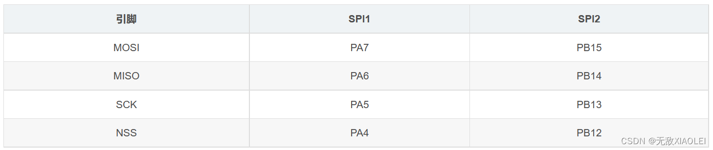 其中SPI1是APB2上的设备,最高通信速率达36Mbits/s(72M/2)。 SPI2是APB1上的设备,最高通信速率达18Mbits/s(36M/2)。
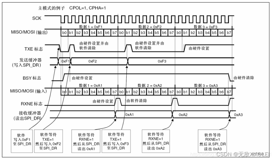 主模式收发流程及事件说明如下: 控制 NSS信号线,产生起始信号(图中没有画出); 把要发送的数据写入到“数据寄存器 DR”中,该数据会被存储到发送缓冲区; 通讯开始,SCK时钟开始运行。MOSI把发送缓冲区中的数据一位一位地传输出去;MISO 则把数据一位一位地存储进接收缓冲区中; 当发送完一帧数据的时候,“状态寄存器 SR”中的“TXE 标志位”会被置 1,表示传输完一帧,发送缓冲区已空;类似地,当接收完一帧数据的时候,“RXNE标志位”会被置 1,表示传输完一帧,接收缓冲区非空; 等待到“TXE标志位”为 1 时,若还要继续发送数据,则再次往“数据寄存器DR”写入数据即可;等待到“RXNE标志位”为 1时,通过读取“数据寄存器DR”可以获取接收缓冲区中的内容。
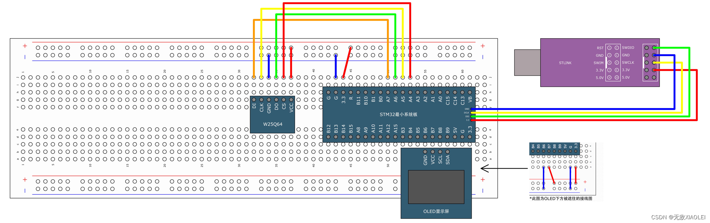
【本文地址】